Digital logic design is an essential part of electronics and computing, and one of the foundational building blocks is the adder. Among the different types of adders, the full adder plays a critical role in performing binary arithmetic. It takes into account the carry from the previous stage, allowing accurate multi-bit addition. The use of XOR gates in implementing full adders has become common because of their efficiency and simplicity. Understanding how to build a full adder using XOR is fundamental for students, hobbyists, and professionals interested in digital electronics and embedded systems.
What Is a Full Adder?
A full adder is a combinational logic circuit that adds three binary bits: two significant bits and a carry-in bit. The output consists of a sum bit and a carry-out bit. This allows cascading multiple full adders to perform addition on binary numbers of any length. The basic truth table of a full adder is defined as follows:
Full Adder Truth Table
- Inputs: A, B, Cin (carry-in)
- Outputs: Sum, Cout (carry-out)
| A | B | Cin | Sum | Cout |
|---|---|---|---|---|
| 0 | 0 | 0 | 0 | 0 |
| 0 | 0 | 1 | 1 | 0 |
| 0 | 1 | 0 | 1 | 0 |
| 0 | 1 | 1 | 0 | 1 |
| 1 | 0 | 0 | 1 | 0 |
| 1 | 0 | 1 | 0 | 1 |
| 1 | 1 | 0 | 0 | 1 |
| 1 | 1 | 1 | 1 | 1 |
Understanding XOR Logic
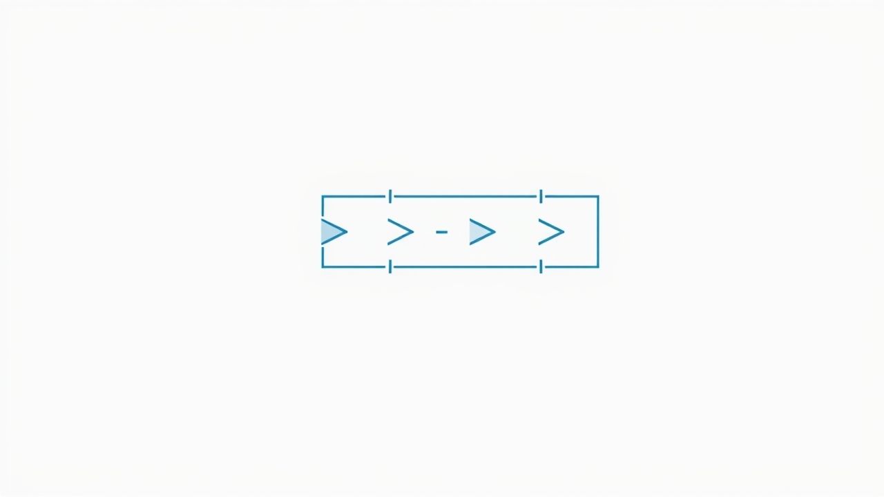
The XOR (exclusive OR) gate is a digital logic gate that outputs true only when the number of true inputs is odd. In the context of binary values, this means:
- 0 XOR 0 = 0
- 0 XOR 1 = 1
- 1 XOR 0 = 1
- 1 XOR 1 = 0
The XOR gate is particularly useful for implementing the sum logic in adders because it naturally handles the toggling behavior needed in binary addition.
Full Adder Using XOR Gates
A full adder can be constructed using two XOR gates, two AND gates, and one OR gate. The logic can be broken down into two stages:
Step-by-Step Logic Breakdown
- First, compute A XOR B using an XOR gate. Let’s call this result ‘X’.
- Next, compute the sum using X XOR Cin. This gives the final sum output.
- For the carry-out, compute (A AND B) and (X AND Cin). OR these two results to get the final carry-out.
This can be represented by the following logic equations:
- Sum = A ⊕ B ⊕ Cin
- Cout = (A AND B) OR ((A ⊕ B) AND Cin)
Circuit Design and Components
To build a full adder using XOR, the following components are typically needed:
- 2 XOR gates
- 2 AND gates
- 1 OR gate
Logical Block Diagram
1. Inputs A and B go into the first XOR gate. 2. The output of that gate goes into the second XOR gate along with Cin. 3. A and B are also connected to the first AND gate. 4. The output of the first XOR gate and Cin go into the second AND gate. 5. Outputs from both AND gates are connected to the OR gate to produce Cout. 6. The output from the second XOR gate is the Sum.
Why XOR Is Ideal for Adders
XOR gates are efficient in representing binary addition logic because of their properties. They allow the toggling of bits, which is essential in binary operations. Additionally, XOR gates are easy to implement in both hardware and software simulations, making them suitable for building more complex arithmetic units.
Advantages of XOR in Full Adder Designs
- Simplifies logic circuit design
- Reduces component count in some cases
- Supports scalable multi-bit adder circuits
- Faster performance in FPGA and ASIC implementations
Application in Multi-Bit Binary Addition
By combining several full adder units using XOR, one can create a ripple carry adder that performs binary addition on larger numbers. For example, a 4-bit binary adder will use four full adder circuits in sequence. The carry-out of one stage becomes the carry-in of the next, and so on. Using XOR in each stage ensures consistent sum computation with minimal delay.
Common Use Cases
Full adders using XOR logic are found in a variety of digital systems, including:
- ALUs (Arithmetic Logic Units)
- Digital signal processors
- Microcontrollers and microprocessors
- Computer arithmetic circuits
- Custom FPGA and ASIC designs
Implementation in VHDL or Verilog
For students and engineers working on hardware description languages, the XOR-based full adder logic is straightforward to translate into code. Here’s an example of the sum and carry logic in Verilog:
assign sum = a ^ b ^ cin;assign cout = (a & b) | ((a ^ b) & cin);
This simplicity in coding and simulation makes XOR-based full adders highly preferred for educational and practical designs alike.
Building a full adder using XOR gates is an essential concept in digital electronics. It introduces learners to binary arithmetic, logic gate functions, and combinational circuit design. XOR gates are not only fundamental in achieving efficient sum computation, but they also provide the flexibility needed in building more complex systems like ripple carry adders and ALUs. Whether used in practical hardware design or in simulation environments, the XOR-based full adder is a foundational element every electronics enthusiast should understand thoroughly.